Sunao Shimizu, Junichi Shiogai, Nayuta Takemori, Shiro Sakai, Hiroaki Ikeda, Ryotaro Arita, Tsutomu Nojima, Atsushi Tsukazaki, and Yoshihiro Iwasa
Journal:Nature Communications
DOI:10.1038/s41467-019-08784-z
Published online: February 18, 2019
Press release online (in Japanese): PDF 444KB
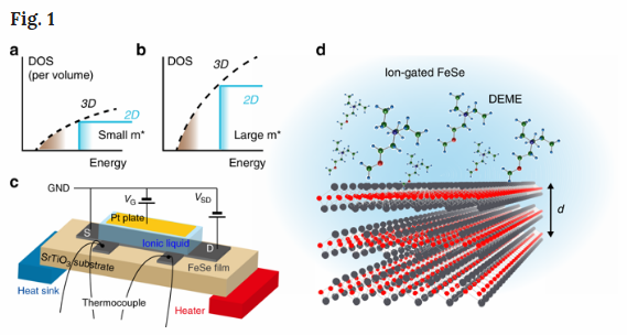
Schematic device structure for thermoelectric measurement. a Schematic illustration of the electronic density of states (DOS) for three-dimensional (3D) and two-dimensional (2D) electrons. b The large effective mass m* enhances the DOS, which is favorable to the enhancement of the Seebeck effect. c Device structure for thermoelectric measurement. VSDand VG stand for the source (S)−drain (D) voltage and the gate bias voltage, respectively. When VG is applied to the Pt plate, ions in the ionic liquid are redistributed, forming an electric double layer on the surface of the FeSe film. d Enlarged illustration of the ionic liquid/FeSe interface. Under the positive gate bias, N,N-diethyl-N-(2-methoxyethyl)-N-methylammonium cations, DEME + , align on the surface of FeSe. The thickness d of the FeSe thin film was tuned by electrochemical etching15. See Methods for details of the device structure and fabrication(From Giant thermoelectric power factor in ultrathin FeSe superconductor)