A research group led by Professor Norio Kobayashi and Assistant Professor Terukazu Nishizaki has successfully developed a scanning tunneling microscope (STM) that enables to observe electronic properties of materials at the atomic level under magnetic fields up to 27 T. The STM has been designed for a hybrid magnet that is installed at High Field Laboratory for Superconducting Materials, IMR. The achievement allows a direct observation of superconducting, magnetic and semiconducting properties with the atomic resolution under the world's highest magnetic field that is much higher than previous observations up to 14 T. The new technology is expected to help clarify a mechanism of high-temperature superconductors and put them into practical use as energy-saving materials in the 21st century. The research results were presented at the 65th Annual Meeting of Physical Society of Japan, and reported in news paper (Nikkei Sangyo Shimbun, on March 16, 2010).
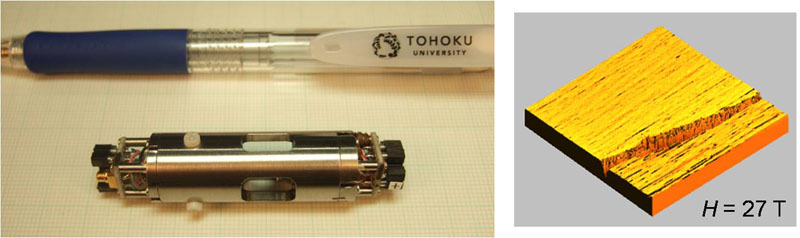
(Left) High-field scanning tunneling microscope.
(Right) Atomic step structure of graphite observed in the hybrid magnet (27T).